What you’ll learn:
Electronic design has always been an endeavor involving a great deal of integration, with much of it being done at the board level. These complex circuit boards require a great deal of testing, during both design and manufacturing, and must be performed by both humans and automated testing systems. To best conduct this testing, the board must be prepared with features that are accessible with a test probe, called test points—their inclusion in printed-circuit-board (PCB) designs is crucial. Testo Probe
Test points have been around for a while, but their modest role continues to expand in today’s crowded boards dominated by surface-mount (SMT), ball-grid-array (BGA), and land-grid-array (LGA) devices, which are hard to access from the sides or top. Facilitating the connection of test probes and test fixtures to the board, test pins help verify the functionality of new components, troubleshoot malfunctioning components, or recalibrate the device or component involved. Differentiated by the type of circuit that they interface with, such pins may be specified as a SMT test point or through-hole test point.
Two primary types of testing require a PCB test point: bench testing by a technician, or automated testing during manufacturing. In a design-for-test approach, designing test points will streamline the PCB testing process and improve tasks that happen in later stages of production. Automated test points on a circuit board can be through-hole pins, vias, or small landing pads of metal designed to accommodate the probes of automated test systems.
Several different board-level tests can be performed, and each is able to be optimized with the right test-point approach. A bare-board test is run after fabrication of the circuit board to make sure that all of the nets in the board have electrical connectivity.
An in-circuit test (ICT) is performed once the board has been assembled. It’s usually positioned on an ICT fixture that’s filled with probes for each individual net, testing the top, bottom, or both sides together if needed. And a flying-probe test is run after assembly on each net of the board by accessing the test points. The flying-probe equipment uses multiple probes that move around to each test point, instead of applying stationary probes in a fixture like ICT.
Manual testing can be performed by a technician or engineer at any time, usually during design development and prototyping. Automated testing is essential for verifying the PCBs during manufacturing, using ICT and flying-probe tests to verify the board assembly and solder connections.
ICT uses a test fixture prepared exclusively for a specific circuit board design; it includes the software that will be run on the test system. The fixture and software are created using the test-point locations and other design data, and a probe is employed for each net in the design. While the main purpose of ICT is to verify the board’s assembly by testing each net for a good connection to its associated part pin, it can also be used to test board functionality.
ICT test fixtures and software are expensive and time-consuming to create. The fixtures involved are complex with thousands of probes, so any changes to a fixture for board revisions can be very expensive. An established in-circuit test can process a large number of circuit boards very quickly. Thus, for mass production, the benefits of speed and functional testing quickly offset the development time and costs.
Flying-probe testing also verifies the integrity of an assembled circuit board, but does so without a test fixture. Instead, several probes fly around, accessing each test point on the board. Since you don’t have to build an expensive test fixture, a flying-probe system can be set up very quickly and inexpensively, and any revisions to the board that require changes to the test system can easily be done.
A disadvantage of flying-probe testing is that the process is very slow, as the system must maneuver the probes around to each individual test point. On a large board, this may take a very long time, without the ability to do functional testing. For prototyping or low-volume production runs, flying-probe testing can be very beneficial.
Of course, there are as many kinds of test points, clips, and pads as there are ways to attach components to a circuit board (see figure). Through-hole test points mount to a PCB’s through holes in the board, and may be specified by the hole diameter, terminal materials, or package type. Common features for through-hole test points include snap-fit mounting and color coding.
Test points are available in a variety of configurations, shapes and styles to perform a variety of specific testing tasks in a device. When it comes to the materials used, most test points are made from a plated strip or wire, cut or stamped into the proper size and shape. Common materials used include brass and phosphor bronze that may be nickel, tin, silver, or gold plated. These materials offer minimal resistance so that when the test points are not in use, they will not affect the functionality of the circuit.
SMT test points are compact terminals soldered to the board, and may also be specified by size, terminal materials, and packaging type. When it comes to the materials used, most test points consist of a plated strip or wire, cut or stamped into the proper size and shape. Common materials include brass and phosphor bronze that may be nickel, tin, silver, or gold plated.
Through-hole mounted (THM) test points, as the name suggests, mount through holes in the PCB. This style of test point can be used in typical wave soldering processes. Typically, these test points are designed with simple legs or pins to go through the board but can have features such as snap-fit legs, orientation pins and designs to keep them perpendicular to the board while being installed. In general, THM test points are manually placed on a board so those additional features available help to ensure stability of the test point in the installation process and use during its life of service.
The shape and style of the “top side” of a THM test can vary greatly based on its functionality. The types of THM test points available include Slotted & Loop Types offering a wide variety of connectivity configurations to suit most design needs. Slotted & Loop type test points are economical choices for reliable PCB test terminations. Terminals are suitable for .062, .093 and .125 thick PC boards. Loop or wire wrap style THM test points use flat phosphor bronze wire offering a large mounting surface. They are also available with colored high temperature insulator bases to enhance visual identification of a circuit.
Surface-mount technology (SMT) test points are soldered directly to a solder pad on the board, allowing them to be installed in the same manner as the components and circuits they are testing with no hole thru the board needed. This allows board designers to use both sides of a PCB for components, increasing the density of a PCB. SMT test points serve the same function as THM test points but offer an alternative board assembly approach. SMT test points are more compact and packaged in bulk like THM test points but more commonly supplied on tape and reel to be compatible with automated pick-and-place technology and standard reflow soldering processes. This makes SMT test points more attractive for larger volume circuit board production.
In deployment, test-point pads and vias are placed along an interconnect or somewhere on a bus as a test point. They could also be used as a via so that inner layers of the PCB are easily accessible. These may be placed along a trace in series, or off to the side as a small stub. Low-speed digital and low-frequency analog signals, even if impedance-controlled, usually don’t pose a signal-integrity problem. Testing high-speed and high-frequency signals requires a test structure with controlled and matched impedances at each port.
It's also a good practice to place an array of test points around any large processor so that all important functionality can be accessed during testing, such as motor drives, low-frequency analog signals, slower digital buses like I2C or SPI, or GPIOs on an MCU. Generally, you can mix and match different types of test points depending on your needs. For in-circuit testing, flying-probe tests, or continuity testing, pads or vias need to be placed on specific points on the board where they can be easily contacted.
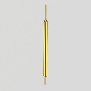
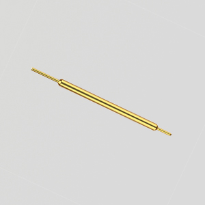
Pogo Pin Contacts Proper test-point placement involves a number of factors. For instance, should test points be deployed on the same side of the PCB, which will impact the testing process? Minimum test point distance is another factor to address testing effectiveness. By distributing test points uniformly across the PCB, it can be more easily tested with multiple probes. Designating an area of your PCB for tall components can also simplify the testing process, ensuring that they don’t hinder access to test points. And don’t forget to consider manufacturing tolerances in the PCB’s initial layout.